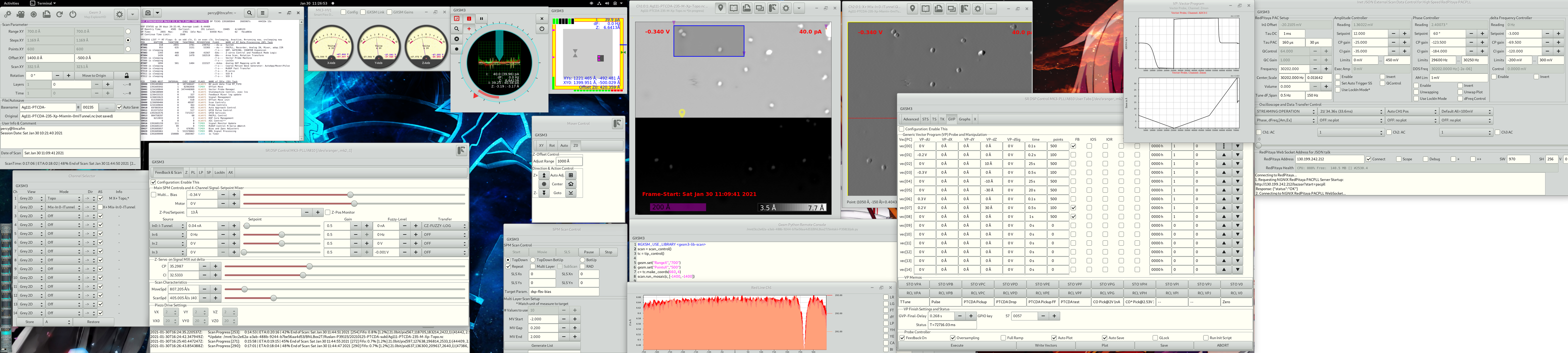
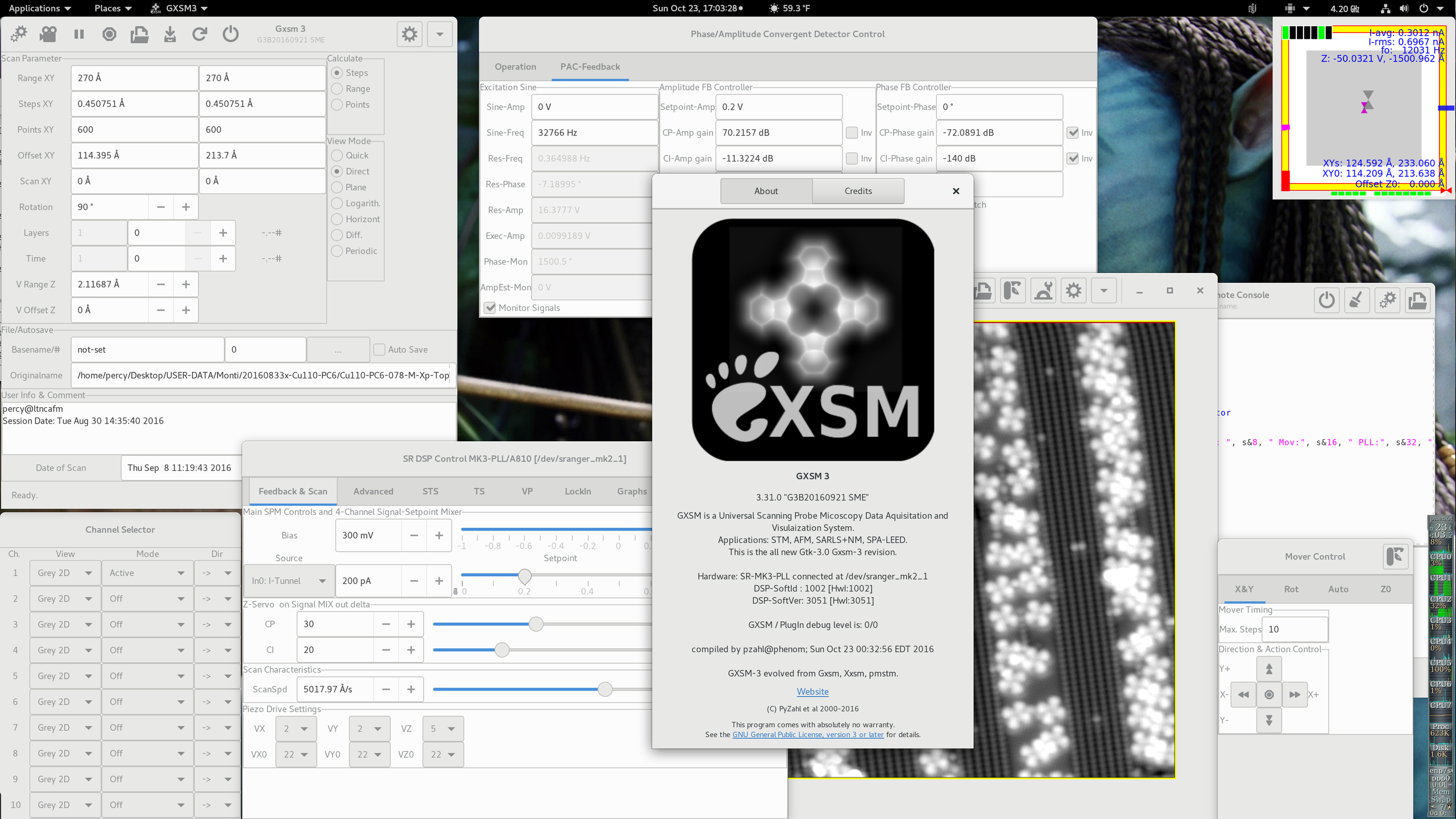
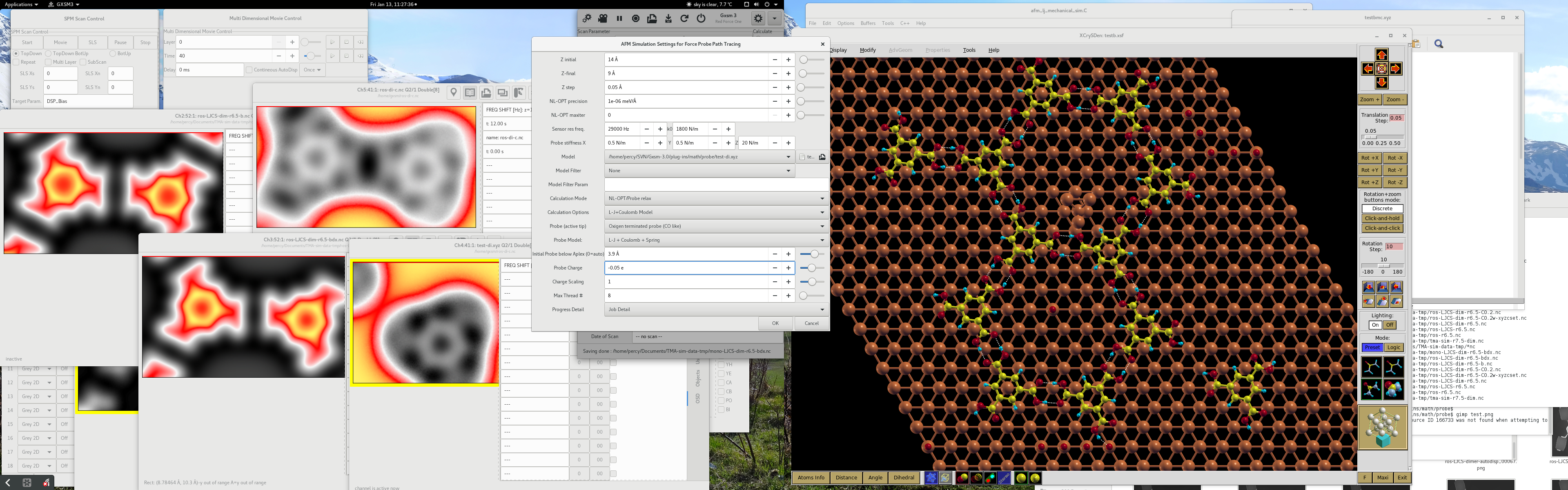
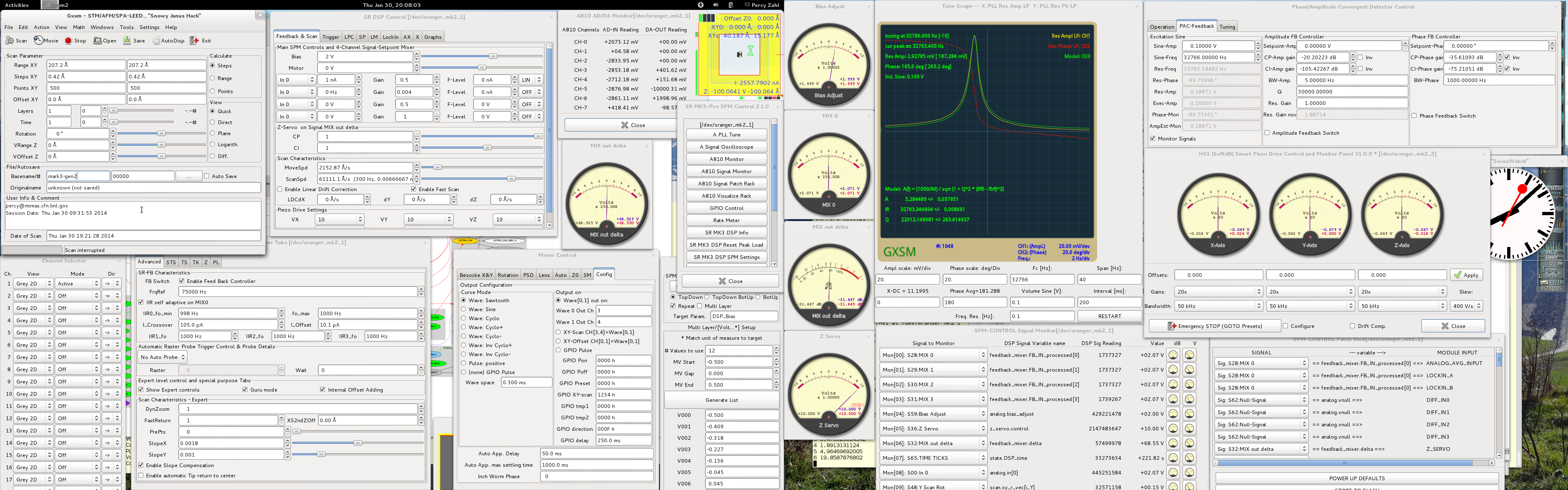
GXSM -- Gnome X Scanning Microscopy: A multi-channel image and vector-probe data acquisition and visualization system designed for SPM techniques (STM,AFM..), but also SPA-LEED/LEED/LEEM data analysis. A plug-in interface allows any user add-on data-processing and special hardware and instrument support. Latest: NC-AFM and related explorative methods as SQDM can be configured. High-Speed external PAC-PLL hardware option with digital DSP link.
Based on several hardware options it supports a commercially available DSP hardware and provided also Open Source Code for all the low level signal processing tasks and instrument controls in a most flexible and adaptable manner.
All latest software is available via SVN only or Live Demo/Install CD: http://www.ventiotec.de/linux/GXSM-Linux.iso
Features
- Scanning Probe Microscopy (and a like)
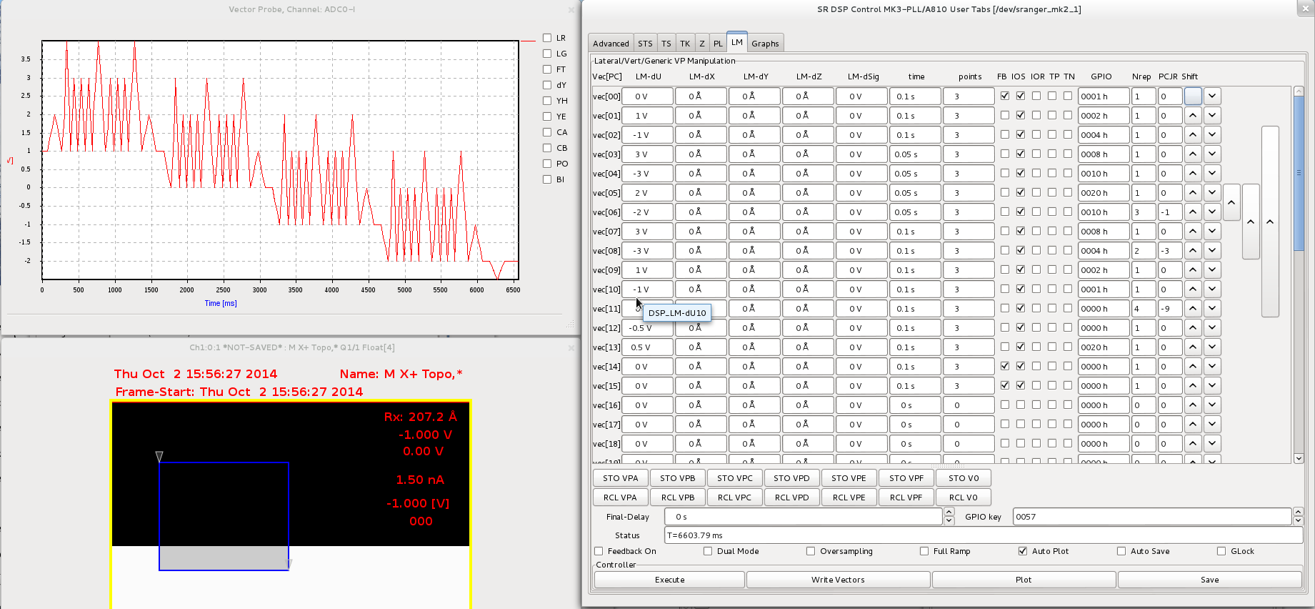
- Modes: STM, AFM (contact), NC-AFM with digital PLL for tuning fork (Q-Plus) like systems (MK3-A810-PLL needed) up to 75kHz (faster with external PLL), ...
- Single DSP based: Multi Channel/Mode Feedback, Scanning, Probing and more
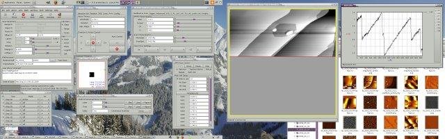
- Multichannel, Multilayerd 2D Data Acquisition and Processing
- Multi Channel, each up to 4D, Data Handling and Visualization
- Multi dimensional Spectroscopic/.. Data Visualization and Analysis
- Multi dimensional data extraction with 1D/2D/3D and volumetric visualizations.
- Real Time (DSP level) Multi Pass Scanning and Probe Data Mapping
- Real Time 3D Visualizations (Open-GL 4.0 based)
- A embedded Python interpreter allows complex scriptable operation
- Integrated High Speed PAC/PLL (125MHz) add on option support via RedPitaya
Project Samples
License
GNU General Public License version 2.0 (GPLv2)Follow GXSM
User Reviews
-
It is an wonderful effort Zahl and Team, your technical contributions are more than developing any social network software. DD
-
STM/SPM and DSPs are our babys since this project's roots dating back to 1995 ;-)